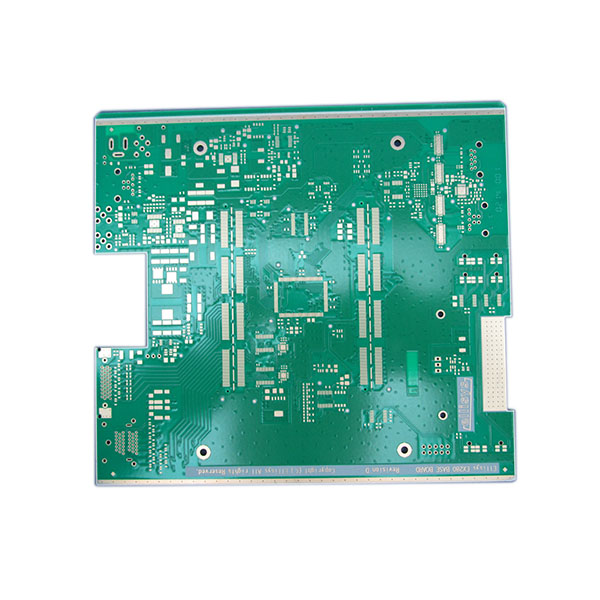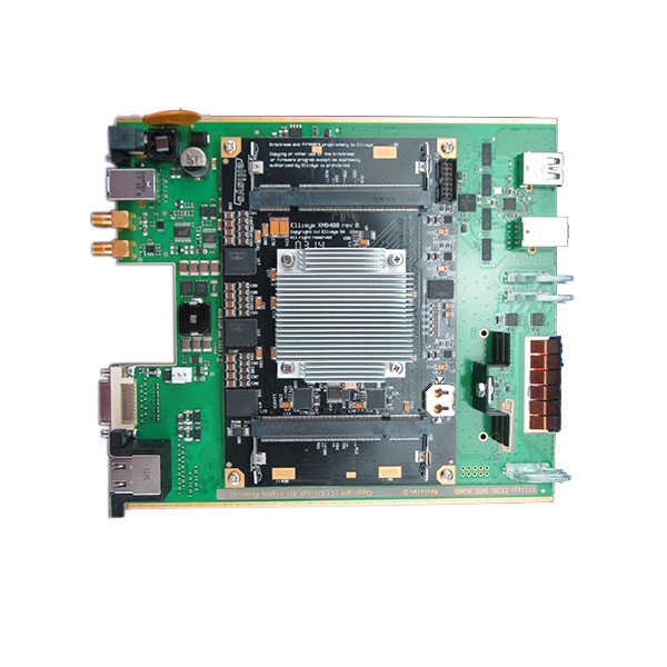


USB Explorer USB 3.0 and 2.0 Test System PCB and PCBA
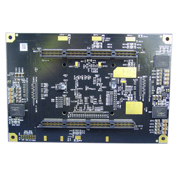
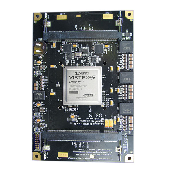
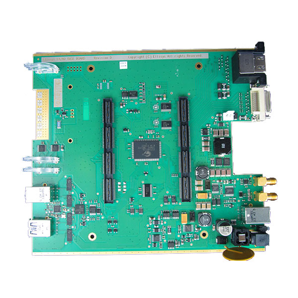
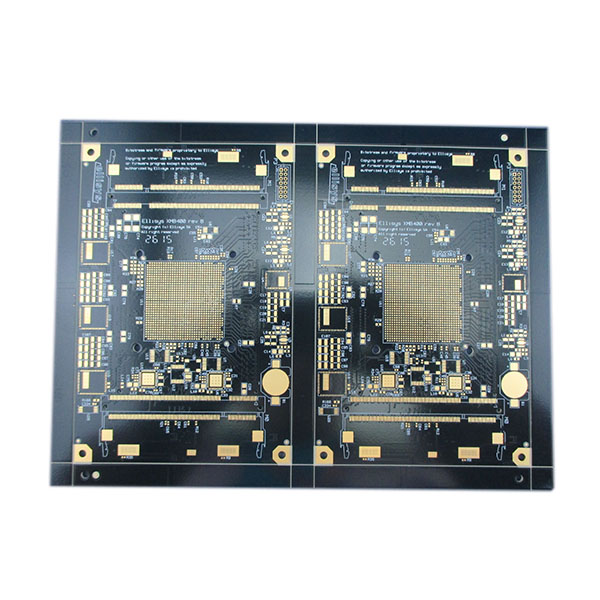
This is a PCB assembly project for USB Explorer USB 3.0 and 2.0 Test System. At Yaheng Circuits, our tester technology understanding make us a unique partner for the instrumentation & measurement business and we are delivering solutions for leading companies in the world.
Product Details
| Layers | 14 layers |
| Board thickness | 1.60 MM |
| Material | PPO/PPE + FR4 high TG 175℃ |
| Copper thickness | 1 OZ(35um) |
| Surface Finish | Immersion Gold; Au Thickness 0.05 um; Ni Thickness 3um |
| Min Hole(mm) | 0.20mm via plugged with solder mask |
| Min Line Width(mm) | 0.13mm |
| Min Line Space(mm) | 0.12mm |
| Solder Mask | Green + Black |
| Legend Color | White |
| Board size | 220*140mm |
| PCB Assembly | Mixed surface mount & through hole assembly |
| RoHS Complied | Lead free assembly process |
| Min components size | 0201 |
| Total components | 1282 per board |
| IC Package | BGA; QFN |
| Main IC | Fairchild, On Semiconductors, Maxim, ADI, Microchip, TI, , Cypress Semi, NXP etc |
| Test | AOI, X-Ray, Functional test |
| Application | Test & measurement |
Our tester technology understanding make us a unique partner for the instrumentation & measurement business and we are delivering solutions for leading companies in the world
> Humidity meters
> Recorders and data loggers
> Spectrum and signal analysis
> Gas analysis
> Density meters
> Non-destructive testing (NDT) equipment
> Diagnostic machines
> Water and environmental test equipment
> Filtration treatment
> Electrical test equipment
> Traffic data recorders
> Metal detection
> And many more
Total process control and reduced tolerances are hugely important for any technology where measurement is the primary product function.
All of the circuit boards manufactured by Yaheng Circuits can be supplied to IPC Class 2 or 3 standards, but more importantly, Yaheng apply tighter tolerance controls that standard to ensure that all products delivered offer continuity of physical dimensions and electronics performance.
The IPC specifications can at times be disconcertingly broad and forgiving for a manufacture of circuit boards, but the difference between top and bottom tolerance can be in the region of 20% variance. Yaheng Circuits feel this is simply not enough control and is completely avoidable if suitable care is taken when selecting raw materials and manufacturing multi-layer PCBs.
For every circuit board supplied by Yaheng Circuit, we supply a several page comprehensive quality report that shows all of the physical dimensions, materials, plating depths and processes confirmation.
The boards are also supplied with a cross section if required to show layer build and internal plating performance, and a solderability sample that indicated the wetting performance of the solderable finish and the PCB’s resistance to delamination.
Every first batch delivered will undergo secondary inspection at the Yaheng Circuits office and each pack is marked with our logo once approved.

